Nvidia aims to run neural nets faster, more efficiently

Artificial intelligence is having a real impact on many industries. It now exceeds humans at some image recognition and speech recognition tasks, it is approaching human levels for language translation, and it is beating experts at all sorts of games. It is being used in medicine, media and entertainment, and security. And autonomous vehicles promise to drastically reduce the 1.3 million road traffic deaths each year--largely through human error.
"Unless you've been sleeping under a rock, you've noticed that there is an AI revolution going on," Bill Dally, Nvidia's Chief Scientist and head of research, said at the recent VLSI Symposia. "Every aspect of human life and commerce is going to be deeply impacted by AI."
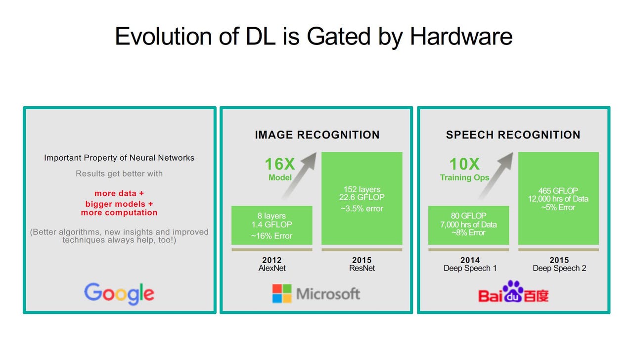
Despite these advances, deep learning remains "completely gated by hardware" because the jobs are getting bigger. ImageNet is now considered a small dataset and some cloud data centers train on more than one billion images and use upwards of 1,000 GPUs, Dally said. Microsoft's ResNet-50 neural network requires 7.72 billion operations to process one low-resolution (225x225) image. In his talk, Dally discussed some of the way that circuit design can increase efficiency of training and inference to meet these growing requirements.
The arithmetic in deep neural networks largely consists of convolutions and matrix multiplication. Training requires at least half-precision (FP16) and the "state-of-the-art," Dally said, is the Tesla V100 with its Tensor Cores that deliver 120 trillion operations per second with very high efficiency. CPUs and FPGAs are orders of magnitude off, he said, and even custom chips would deliver at best 30 percent better performance per watt.
The V100 is also at the heart of what is now the world's fastest supercomputer. Summit has 4,608 nodes each with two IBM Power9 CPUs and six Tesla V100s for a total of 27,648 GPUs and is theoretically capable of three exaops of peak throughput (the official measure is 122.3 petaflops on High Performance Linpack). Dally said Oak Ridge National Laboratory has already run simulations that can sustain 1.6 exaops on "meaningful applications."
Running these trained models is different. For inference, the accuracy you get at INT8 is "plenty" and reduced precision saves energy because matrix multiplication increases quadratically and it also reduces die area (and therefore cost). The Xavier SoC, which is basically one-tenth of a V100 but with a fixed-function deep-learning accelerator like Google's TPU, can deliver up to 20 trillion operations per second. Noting that Google compared its TPU to an older Nvidia K80, Dally said the Pascal-based Tesla P40 already delivers better performance for inference.
The challenge for inference is to handle lots of operations in real-time using the minimum amount of energy. For example, Nvidia's DriveNet has 12 cameras that run through four separate neural networks. At HD resolution, it requires 9.4 trillion operations per second per image. "This is an enormous computation load that is being done in a vehicle where power is limited," Dally said. Nvidia developed a method of training networks to do inference down to four bits with little loss in accuracy so that at 16nm core inference operations (MAC) can be performed in about 10 femtojoules digitally, "and I actually think you can do better than that."
When you drive the math down to that level, the challenges are all about moving data around. Accessing local SRAM consumes 5 picojoules per word, on-chip cache uses 50 picojoules, and going out to low-power DDR DRAM (or high-bandwidth memeory) is 640 picojoules, "so you don't want to have to go off chip." At 10 femtojoules, the cost of computation is so low that even pulling data from SRAMs starts to dominate. Dally suggested some techniques for reducing the cost of communications at three levels: on chip, on module and between modules.
After reducing the precision, the next trick is to take advantage of the data sparsity in most neural network models. Nvidia has previously presented a three-step process that consists of training the network to learn which connections are important, pruning the unimportant parameters, and then retraining the network to fine tune the weights of the remaining connections to recover accuracy. By exploiting data reuse in multiply-accumulate operations, the system can minimize memory bandwidth and power.
When you do need to go to memory, the on-chip wires are very dense, but not energy efficient and that's unlikely to improve because supply voltages are scaling very slowly. Nvidia has proposed the idea--first presented at ISSCC--of charge recycled signaling, which uses stacks of wire repeaters to get a four-fold improvement in on-chip energy efficiency. To avoid interference, Nvidia borrows the concept of balancing traffic on parallel wires--typically used in semi-custom fabrics to traverse longer distances--to create a network-on-chip fabric that consumes only one square millimeter of die area and has a bandwidth of 4TB per second.
At the module level, Dally talked about an array that consists of four GPUs surrounded by stacks of DRAM memory. These multi-chip modules also require signaling that is dense and energy efficient. Each GPU requires one terabit per second of DRAM bandwidth--a number that scales with GPU performance--and the GPUs need to be connected to one another with comparable bandwidth. Since each chip has only a few hundred usable signal pins on each edge, you need signaling rates of 20Gbps or more to reach this level of throughput. Conventional SerDes links use a lot of power, but Nvidia has been experimenting with a technology called ground-referenced signaling (GRS) that Dally said operates reliably at speeds up to 25bps while using about 20 percent of the power. GRS could be used to connect multiple chips in a single module or to connect multiple packages spaced closely together on a printed circuit board.
At the top level, Nvidia talked about a more efficient way to connect multiple modules. To train a large model such as ResNet-50, each GPU needs about 400GB per second of I/O bandwidth to exchange parameters. The conventional approach using striplines and through-hole vias in printed circuit boards to route high-speed data between modules uses 10 to 15 picojoules per bit. Instead Nvidia proposed packaging the modules closely together with liquid cooling and then connecting them directly with flexible printed-circuit board links. When signaling at 25Gbps, 40mm of package edge can support 400- to 500GBps of I/O bandwidth per GPU while using just two picojoules per bit.
Whether Nvidia will adopt any of these research ideas in future accelerators and DGX systems isn't clear. What is apparent, however, is that the industry can no longer count on Moore's Law to deliver the same performance improvements every couple of years. As raw computation reaches its limits in terms of performance per watt, the cost of moving data around has become the bottleneck and it will take some creative ideas at all levels of system design to continue to scale artificial intelligence.